
Classic 8 bit parts

Classic 8 bit Device Library
To support the development of retro computer systems I have implemented a variety of classic 8 bit devices in Verilog suitable for synthesis into FPGAs.
MOS 6502
One of the most popular CPUs of the home computer era and still going strong today. This is an implementation of the MOS semiconductor 6502 CPU. This design models the original NMOS 6502 behaviour. It implements all valid instructions, with invalid opcodes being mapped to the no operation NOP opcode. To give a degree of confidence in the design it has been validated against the Klaus Dormann suite of tests which can be found on github here.

cpu6502
This is the top level module which instantiates the three sub modules and connects them together. It also implements the Accumulator, X and Y index registers, the Flags register and the Stack pointer. Logic to detect and handle IRQ, NMI and BRK events is also in this module
ALU - Arithmetic Logic Unit
This is a combinatorial block which models the 6502 cpu instructions. When the alu_execute signal is asserted a large case structure is used to provide for each instruction a set of outputs based on the ALU inputs. Every instruction is represented and the actions for it specified. BCD addition and subtraction have been added outside of the case statement for clarity as multiple steps are needed for these instructions.
IDC - Instruction Decode
This is a combinatorial block which decodes the incoming opcode into a 6502 instruction that can be processed by the ALU and the memory interface unit. All invalid opcodes are set to NOP.
MEMIF - Memory Interface
This block is the main part of the design. A large state machine is used to read an opcode from memory and then execute it with support of the ALU and IDC modules. The state machine implements all of the addressing modes for every instruction and the flow of operations to implement every instruction. The program counter can be found in this module along with support registers to store intermediate values read from memory during the execution of the instruction.
When writing to memory the address is presented, write data is output on mem_data_o and the mem_wr strobe is asserted. Data should be accepted by external memory in this cycle. When reading from memory the address is presented and the mem_rd strobe is asserted. Data should be provided by external memory on the mem_data_i port in the next cycle. Both read and write accesses are compatible with standard clocked FPGA memory blocks.
Motorola 6847
The Motorola 6847 was an early video display generator released in 1978. It found its way into many computer systems, notably the Dragon 32, Tandy Colour Computer and Acorn Atom as well as a host of lesser known machines such as the Laser 200. It could generate a rather low density 32x16 text screen, simple semigraphics modes and a range of 2 or 4 colour pixel graphics modes of varying resolutions. It claimed a range of 9 colours but was very restrictive on how these colours could be used resulting in rather unappealing four colour images featuring red,yellow,blue and green or buff,magenta,cyan and orange.
More details on the 6847 can be found on wikipedia.
My 6847 design implements all of the modes of the original device except support for an external character rom. It works with a VGA timing block to generate a 256x192 image (pixels doubled vertically and horizontally) in a standard 640x460 VGA image. I used my existing character display 5000 block as the basis for this design, simplifying the logic to match the reduced complexity of the 6847.
Text mode showing the two main text colours.

Semigraphics mode - Semigraphics-4 in the top half which allows all 9 colours with a 64x32 block resolution and Semigraphics-6 in the bottom half which allows 4 colours with a 'higher' resolution of 64x48 blocks.
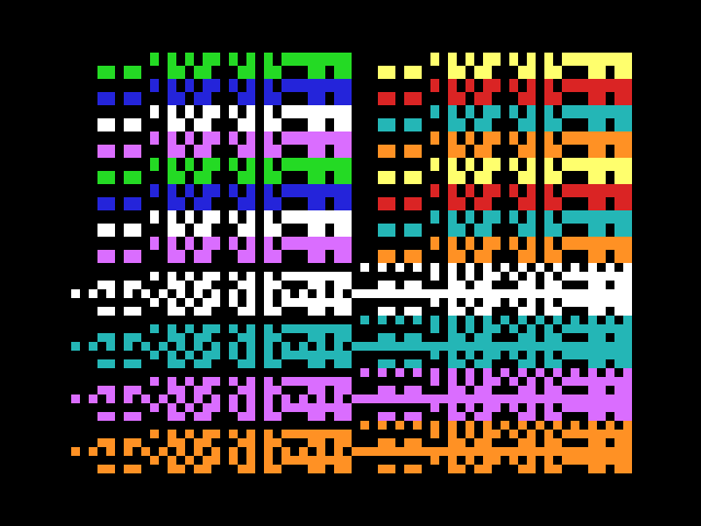
Four colour pixel mode in the classic red,yellow,blue and green palette.
